
Nonetheless, though laptop or computer chips will not burn off a literal gap in your pocket (nevertheless they do get warm sufficient to
fry an egg), they nonetheless demand a great deal of existing to run the purposes we use just about every working day. Consider the facts-centre SoC: On ordinary, it truly is consuming 200 W to provide its transistors with about one to two volts, which usually means the chip is drawing one hundred to 200 amperes of existing from the voltage regulators that source it. Your regular fridge draws only 6 A. Significant-conclude cell telephones can draw a tenth as much energy as facts-centre SoCs, but even so that’s nonetheless about 10–20 A of existing. That’s up to 3 fridges, in your pocket!
Delivering that existing to billions of transistors is swiftly getting to be one particular of the key bottlenecks in large-general performance SoC design and style. As transistors go on to be made tinier, the interconnects that source them with existing ought to be packed at any time nearer and be made at any time finer, which will increase resistance and saps energy. This can not go on: Without having a major adjust in the way electrons get to and from products on a chip, it will not issue how much more compact we can make transistors.
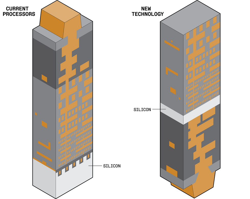
In today’s processors each alerts and energy get to the silicon [mild gray] from higher than. New technological know-how would separate those people features, saving energy and building much more place for sign routes [appropriate].Chris Philpot
The good thing is, we have a promising alternative: We can use a facet of the silicon that’s very long been disregarded.
Electrons have to journey a very long way to get from the resource that is building them to the transistors that compute with them. In most electronics they journey along the copper traces of a printed circuit board into a bundle that retains the SoC, through the solder balls that hook up the chip to the
bundle, and then by means of on-chip interconnects to the transistors on their own. It truly is this previous stage that genuinely issues.
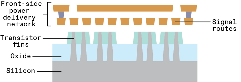
To see why, it assists to fully grasp how chips are made. An SoC starts off as a bare piece of large-excellent, crystalline silicon. We to start with make a layer of transistors at the really top rated of that silicon. Up coming we hyperlink them together with metal interconnects to kind circuits with helpful computing features. These interconnects are shaped in layers named a stack, and it can just take a 10-to-twenty-layer stack to produce energy and facts to the billions of transistors on today’s chips.
All those layers closest to the silicon transistors are thin and compact in get to hook up to the small transistors, but they expand in sizing as you go up in the stack to bigger levels. It truly is these levels with broader interconnects that are better at offering energy simply because they have less resistance.
These days, each energy and alerts get to transistors from a community of interconnects higher than the silicon (the “entrance facet”). But increasing resistance as these interconnects are scaled down to at any time-finer dimensions is building that scheme untenable.Chris Philpot
You can see, then, that the metal that powers circuits—the energy supply community (PDN)—is on top rated of the transistors. We refer to this as entrance-facet energy supply. You can also see that the energy community unavoidably competes for area with the community of wires that delivers alerts, simply because they share the very same established of copper assets.
In get to get energy and alerts off of the SoC, we generally hook up the uppermost layer of metal—farthest away from the transistors—to solder balls (also named bumps) in the chip bundle. So for electrons to get to any transistor to do helpful perform, they have to traverse 10 to twenty layers of more and more slender and tortuous metal till they can finally squeeze through to the really previous layer of neighborhood wires.
This way of distributing energy is basically lossy. At just about every stage along the path, some energy is misplaced, and some ought to be employed to command the supply itself. In today’s SoCs, designers generally have a budget that will allow loss that leads to a 10 percent reduction in voltage among the bundle and the transistors. Therefore, if we strike a full performance of ninety percent or increased in a energy-supply community, our patterns are on the appropriate track.
Historically, such efficiencies have been achievable with good engineering—some may possibly even say it was simple as opposed to the issues we confront nowadays. In today’s electronics, SoC designers not only have to take care of increasing energy densities but to do so with interconnects that are losing energy at a sharply accelerating level with each individual new generation.
You can design and style a back again-facet energy supply community that’s up to 7 situations as successful as the classic entrance-facet community.
The increasing lossiness has to do with how we make nanoscale wires. That procedure and its accompanying elements trace back again to about 1997, when IBM commenced to make interconnects out of copper rather of aluminum, and the sector shifted along with it. Up till then aluminum wires had been wonderful conductors, but in a number of much more methods along the
Moore’s Legislation curve their resistance would quickly be much too large and become unreliable. Copper is much more conductive at present day IC scales. But even copper’s resistance commenced to be problematic at the time interconnect widths shrank underneath one hundred nanometers. These days, the smallest manufactured interconnects are about twenty nm, so resistance is now an urgent issue.
It assists to picture the electrons in an interconnect as a complete established of balls on a billiards table. Now envision shoving them all from one particular conclude of the table towards an additional. A number of would collide and bounce in opposition to each individual other on the way, but most would make the journey in a straight-ish line. Now think about shrinking the table by half—you’d get a great deal much more collisions and the balls would go much more gradually. Up coming, shrink it all over again and enhance the amount of billiard balls tenfold, and you might be in one thing like the circumstance chipmakers confront now. True electrons really don’t collide, always, but they get shut sufficient to one particular an additional to impose a scattering force that disrupts the stream through the wire. At nanoscale dimensions, this leads to vastly bigger resistance in the wires, which induces sizeable energy-supply loss.
Increasing electrical resistance is not a new problem, but the magnitude of enhance that we are viewing now with each individual subsequent procedure node is unprecedented. Furthermore, classic means of handling this enhance are no for a longer period an alternative, simply because the producing guidelines at the nanoscale impose so numerous constraints. Absent are the times when we could arbitrarily enhance the widths of specific wires in get to combat increasing resistance. Now designers have to adhere to specific specified wire widths or else the chip may possibly not be manufacturable. So, the sector is confronted with the twin complications of bigger resistance in interconnects and less place for them on the chip.
There is an additional way: We can exploit the “empty” silicon that lies underneath the transistors. At Imec, exactly where authors Beyne and Zografos perform, we have pioneered a producing strategy named “buried energy rails,” or BPR. The system builds energy connections underneath the transistors rather of higher than them, with the aim of making fatter, less resistant rails and releasing area for sign-carrying interconnects higher than the transistor layer.
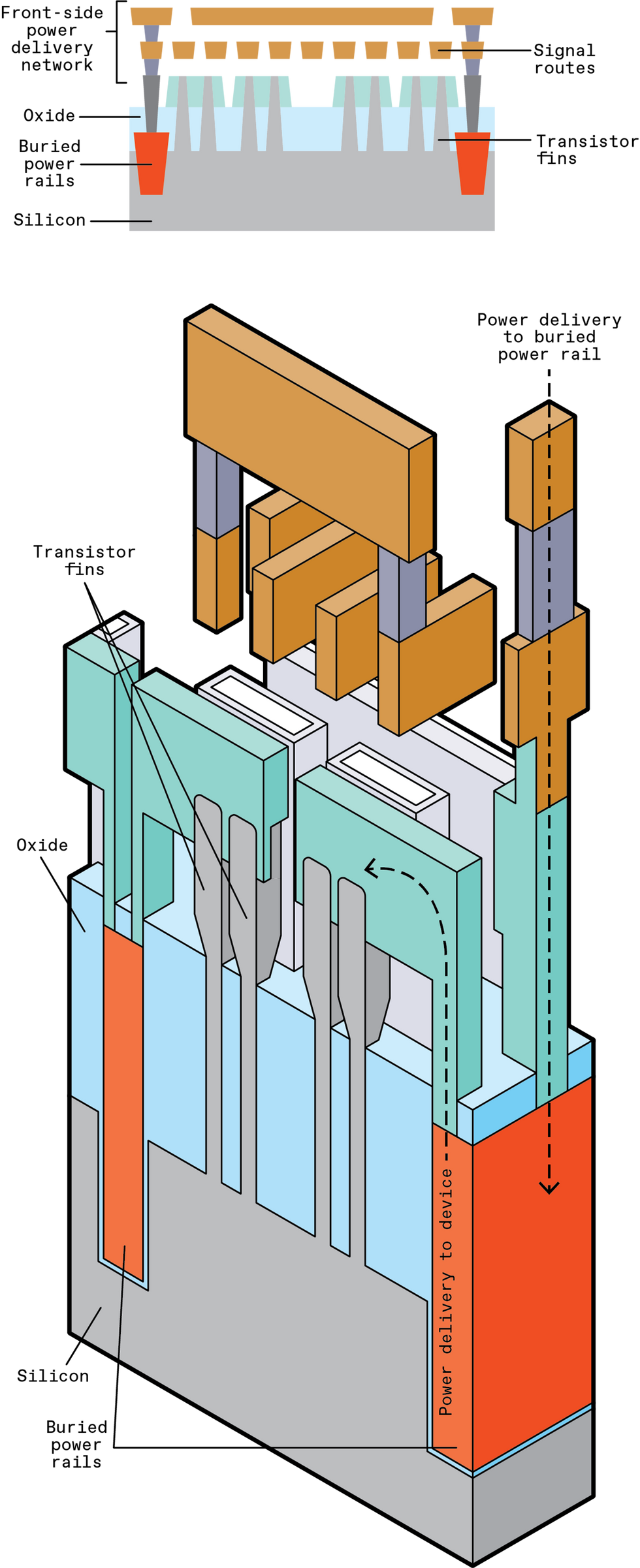
To lessen the resistance in energy supply, transistors will faucet energy rails buried in just the silicon. These are somewhat significant, very low-resistance conductors that many logic cells could hook up with.Chris Philpot
To construct BPRs, you to start with have to dig out deep trenches underneath the transistors and then fill them with metal. You have to do this in advance of you make the transistors on their own. So the metal selection is crucial. That metal will have to have to endure the processing methods employed to make large-excellent transistors, which can get to about one,000 °C. At that temperature, copper is molten, and melted copper could contaminate the complete chip. We have for that reason experimented with ruthenium and tungsten, which have bigger melting points.
Considering the fact that there is so much unused area underneath the transistors, you can make the BPR trenches vast and deep, which is fantastic for offering energy. In comparison to the thin metal layers specifically on top rated of the transistors,
BPRs can have one/twenty to one/30 the resistance. That usually means that BPRs will correctly allow you to produce much more energy to the transistors.
Furthermore, by going the energy rails off the top rated facet of the transistors you free up place for the sign-carrying interconnects. These interconnects kind essential circuit “cells”—the smallest circuit units, such as SRAM memory bit cells or basic logic that we use to compose much more advanced circuits. By using the area we’ve freed up, we could shrink those people cells by
sixteen percent or much more, and that could eventually translate to much more transistors for every chip. Even if element sizing stayed the very same, we would nonetheless force Moore’s Legislation one particular move more.
Sad to say, it looks like burying neighborhood energy rails by yourself will not be sufficient. You nonetheless have to convey energy to those people rails down from the top rated facet of the chip, and that will price performance and some loss of voltage.
Absent are the times when we could arbitrarily enhance the widths of specific wires in get to combat increasing resistance.
Scientists at Arm, like authors Cline and Prasad, ran a simulation on one particular of their CPUs and discovered that, by on their own, BPRs could allow you to construct a 40 percent much more successful energy community than an regular entrance-facet energy supply community. But they also discovered that even if you employed BPRs with entrance-facet energy supply, the in general voltage shipped to the transistors was not large sufficient to maintain large-general performance operation of a CPU.
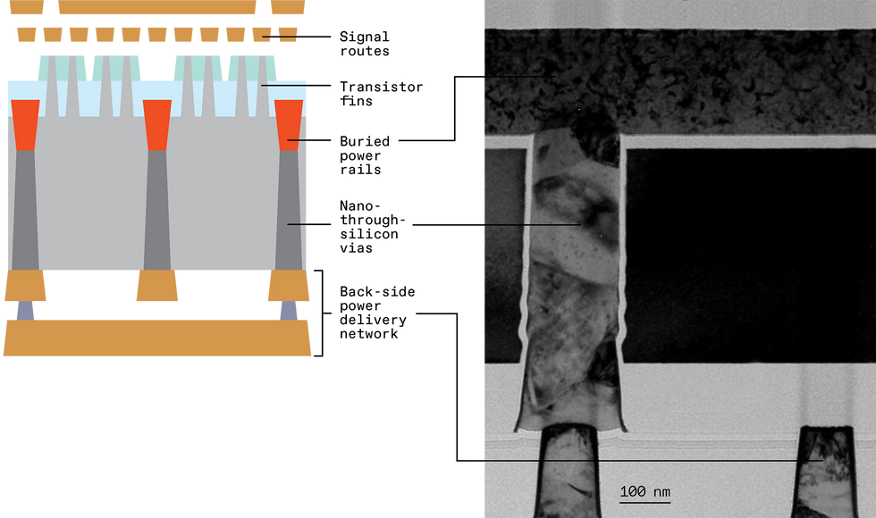
The good news is, Imec was concurrently building a complementary alternative to more improve energy supply: Transfer the complete energy-supply community from the entrance facet of the chip to the back again facet. This alternative is named “back again-facet energy supply,” or much more frequently “back again-facet metallization.” It consists of thinning down the silicon that is beneath the transistors to 500 nm or less, at which stage you can create nanometer-sizing “through-silicon vias,” or
nano-TSVs. These are vertical interconnects that can hook up up through the back again facet of the silicon to the base of the buried rails, like hundreds of small mineshafts. As soon as the nano-TSVs have been produced underneath the transistors and BPRs, you can then deposit added layers of metal on the back again facet of the chip to kind a total energy-supply community.
Expanding on our previously simulations, we at Arm discovered that just two layers of thick back again-facet metal was sufficient to do the occupation. As very long as you could area the nano-TSVs nearer than two micrometers from each individual other, you could design and style a back again-facet PDN that was 4 situations as successful as the entrance-facet PDN with buried energy rails and 7 situations as successful as the classic entrance-facet PDN.
The back again-facet PDN has the added advantage of staying physically separated from the sign community, so the two networks no for a longer period compete for the very same metal-layer assets. There’s much more place for each individual. It also usually means that the metal layer traits no for a longer period have to have to be a compromise among what energy routes want (thick and vast for very low resistance) and what sign routes want (thin and slender so they can make circuits from densely packed transistors). You can concurrently tune the back again-facet metal layers for energy routing and the entrance-facet metal layers for sign routing and get the ideal of each worlds.
Going the energy supply community to the other facet of the silicon—the “back facet”—reduces voltage loss even much more, simply because all the interconnects in the community can be made thicker to reduced resistance. What is actually much more, taking away the energy-supply community from higher than the silicon leaves much more place for sign routes, major to even more compact logic circuits and allowing chipmakers squeeze much more transistors into the very same spot of silicon.
Chris Philpot/IMEC
In our patterns at Arm, we discovered that for each the classic entrance-facet PDN and entrance-facet PDN with buried energy rails, we had to sacrifice design and style general performance. But with back again-facet PDN the CPU was able to obtain large frequencies
and have electrically successful energy supply.
You may possibly, of class, be pondering how you get alerts and energy from the bundle to the chip in such a scheme. The nano-TSVs are the critical right here, much too. They can be employed to transfer all input and output alerts from the entrance facet to the back again facet of the chip. That way, each the energy and the I/O alerts can be attached to solder balls that are placed on the back again facet.
Simulation studies are a fantastic start off, and they display the CPU-design and style-degree prospective of back again-facet PDNs with BPR. But there is a very long street ahead to carry these systems to large-volume producing. There are nonetheless sizeable elements and producing issues that have to have to be solved. The ideal selection of metal elements for the BPRs and nano-TSVs is essential to manufacturability and electrical performance. Also, the large-factor-ratio (deep but skinny) trenches wanted for each BPRs and nano-TSVs are really complicated to make. Reliably etching tightly spaced, deep-but-slender attributes in the silicon substrate and filling them with metal is somewhat new to chip manufacture and is nonetheless one thing the sector is finding to grips with. Building producing tools and techniques that are trusted and repeatable will be essential to unlocking common adoption of nano-TSVs.
Furthermore, battery-powered SoCs, like those people in your telephone and in other energy-constrained patterns, already have much much more refined energy-supply networks than those people we’ve mentioned so significantly. Fashionable-working day energy supply separates chips into many energy domains that can operate at various voltages or even be turned off entirely to conserve energy. (See ”
A Circuit to Improve Battery Lifetime,” IEEE Spectrum, August 2021.)
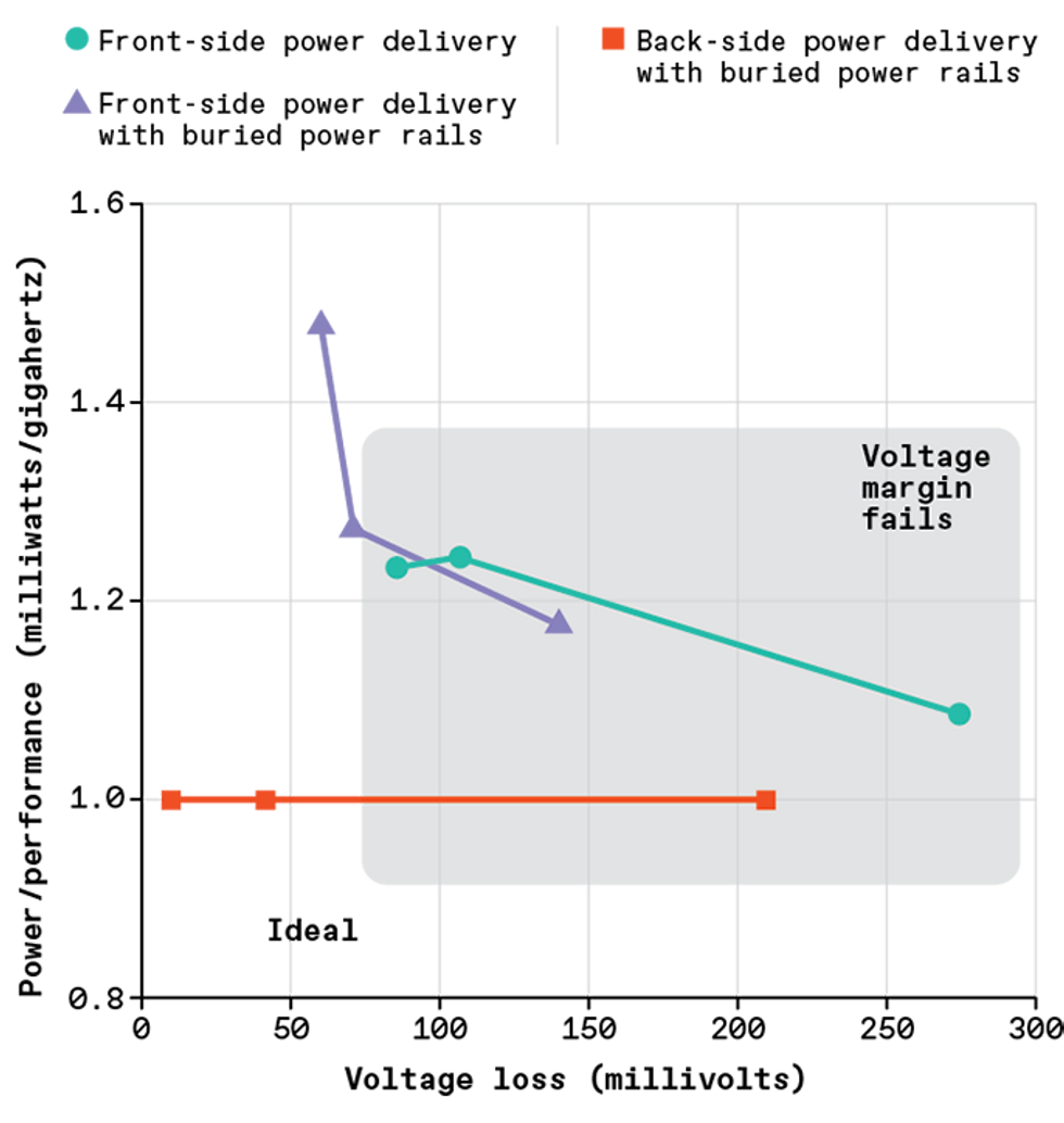
In tests of many patterns using 3 types of energy supply, only back again-facet energy with buried energy rails [red] gives sufficient voltage with no compromising general performance.Chris Philpot
Therefore, back again-facet PDNs and BPRs are sooner or later likely to have to do much much more than just successfully produce electrons. They are likely to have to exactly command exactly where electrons go and how numerous of them get there. Chip designers will not want to just take many methods backward when it arrives to chip-degree energy design and style. So we will have to concurrently optimize design and style and producing to make absolutely sure that BPRs and back again-facet PDNs are better than—or at least suitable with—the energy-saving IC techniques we use nowadays.
The future of computing is dependent on these new producing techniques. Power intake is important whether you might be worrying about the cooling invoice for a facts centre or the amount of situations you have to demand your smartphone each individual working day. And as we go on to shrink transistors and ICs, offering energy results in being a sizeable on-chip problem. BPR and back again-facet PDNs may possibly effectively remedy that problem if engineers can overcome the complexities that occur with them.
This short article appears in the September 2021 print issue as “Power From Below.”
