
Intel is a firm in a spot of bother: TSMC, Apple, and other rivals are outpacing its chip engineering and Moore’s Regulation – actually designed by Intel’s founder – is setting up to bring about the chipmaker some head aches.
Even so a patent unearthed by Twitter consumer @Underfox3 has uncovered that the company could nicely be producing a approach: stacking transistors on major of every single other for greater functionality in less place. Now, of study course, this is only a patent – corporations patent bizarre and whacky factors all the time for a assortment of motives, most probable to avert competitors from having the leap on them.
But there is some thing appealing about Intel thinking its way all over the problem of how to squeeze much more power into at any time-smaller sized areas – particularly, if this style will come to fruition, Intel could be seeking at sub-2 nanometer (nm) processes.
Patent: Stacked Forksheet Transistors – Intel”The blend of shared-gate stacked nanoribbon transistors with a self-aligned dielectric wall can eventually lead to an ultimately scaled 3D stacked forksheet CMOS architecture. (…)”Extra facts: https://t.co/bJjuD7rlRH pic.twitter.com/ZZvYLNAedWJanuary 13, 2022
Intel calls the layout “stacked forksheet transistors” and you can see why: the transitions would be stacked on prime of each and every other.
As Intel clarifies: “A first transistor machine involves a initial vertical stack of semiconductor channels adjacent to an edge of the backbone. A second transistor device includes a next vertical stack of semiconductor channels adjacent to the edge of the backbone. The second transistor gadget is stacked on the 1st transistor unit.”
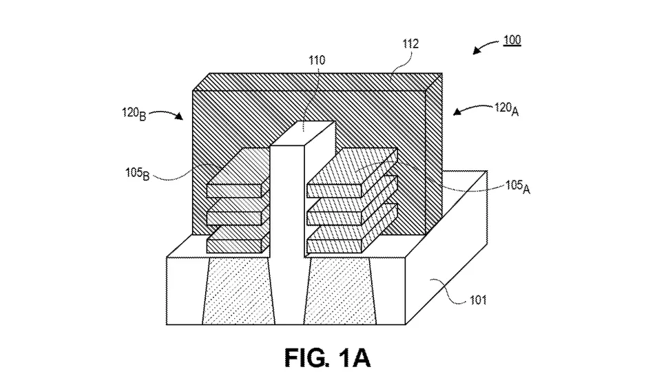
The stop end result from this really nerdy patent software is that Intel could develop a 3D vertically-stacked CMOS architecture, letting for increased transistor counts about today’s present-day architectures – a big enhance for the company. The company does note nevertheless that, as it stands, the constraints are “overpowering”.
It is really impossible to inform specifically what type of efficiency uplift could be realized by Intel’s design, and the company conspicuously would not speculate, but TSMC moving from a 5nm course of action to a 3nm procedure resulted in 10% to 15% effectiveness gains although using up to 30% much less electric power.
Irrespective of whether this patent ever makes it into output or not, it is really interesting to see Intel working via the issue of how to squeeze additional electric power out of much less, in particular as the firm commences its changeover less than new CEO Pat Gelsinger. A sub-2nm approach would be game transforming, placing Intel in-line with Apple’s amazingly amazing M1 series processors.
Via Tom’s Components
